
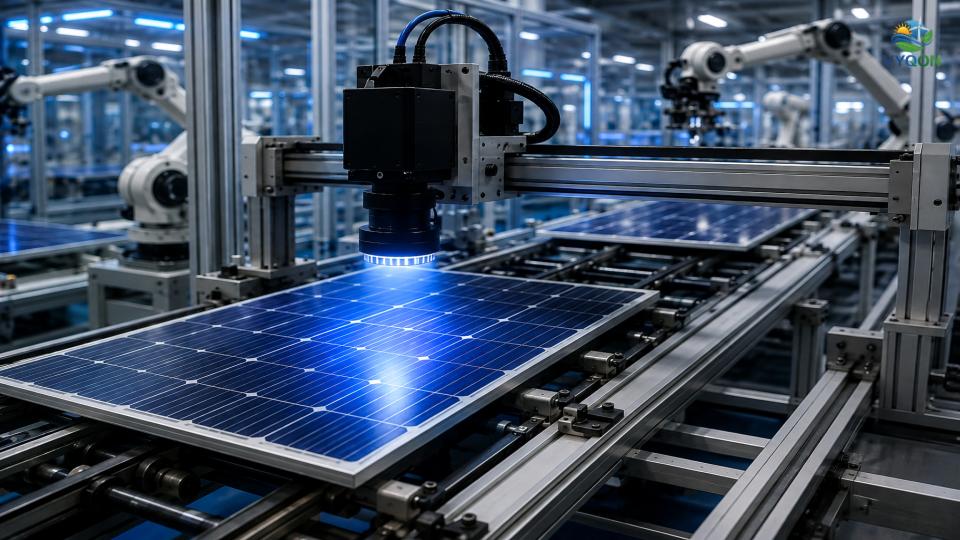
The global photovoltaic industry is scaling at an unprecedented rate, with factory outputs now routinely measured in tens of gigawatts (GW) annually. The sheer speed of production has outpaced traditional quality control methods. Modern solar panel manufacturing operates at the intersection of semiconductor precision and mass production economics. As module architectures become incredibly complex and throughput demands intensify, human inspection is no longer viable.
In 2026, tier-1 factories are aggressively deploying AI in Solar Manufacturing. By integrating deep learning algorithms with advanced Machine Vision, manufacturers are achieving 99.9% defect detection accuracy at millisecond speeds. For project developers and EPCs, this automation guarantees lower degradation rates and highly bankable module batches. Here is how AI is reshaping the factory floor.
The Bottleneck of Manual Quality Assurance
Modern solar assembly lines process thousands of cells per hour. Wafer handling at speeds exceeding 3,000 cells per hour creates significant micro-crack risks. Historically, quality assurance relied on human operators visually inspecting cells for chips, color variations, or alignment errors.
However, at these incredible throughput speeds, a human operator simply cannot detect a microscopic defect on a moving conveyor belt. Furthermore, traditional visual checks might mistake acceptable texture variations for true defects like scratches or contact errors. Relying on manual inspection today results in massive manufacturing bottlenecks, high false-rejection rates, and the critical risk of defective panels making it out into the field where they will ultimately fail. Advanced machine vision solves this challenge by accurately classifying real defects while ignoring normal appearance variations, ensuring that perfectly good cells are not thrown away.
Deep Learning and Electroluminescence (EL) Imaging
The backbone of AI in Solar Manufacturing is its integration with Electroluminescence (EL) imaging. An EL test operates much like an X-ray for a solar panel; an electrical current is passed through the cell, causing the healthy active silicon to emit near-infrared light in the darkness. Cracked or inactive regions stay dark because current cannot reach them.
Machine vision systems capture these EL images and feed them into deep learning neural networks. These AI models have been trained on millions of images to instantly recognize the visual signatures of hidden defects. Within milliseconds, the AI can pinpoint dead pixels, intrinsic silicon impurities, and microscopic microcracks. By processing low-level structures and local brightness variations, the AI progressively transforms defect patterns into highly accurate classifications.
Detecting Microcracks and Encapsulant Voids
As cell architectures become thinner to save on silicon costs, they become increasingly fragile. Hairline fractures from handling, stringing, or lamination are often 10 to 100 microns wide. These cracks are completely invisible to the naked eye and standard optical cameras, meaning they effortlessly slip past conventional visible-light checks.
Beyond the silicon itself, the lamination phase introduces its own set of critical risks. The lamination process must eliminate all encapsulant voids and bubbles without leaving stress concentrations. EVA or POE voids are encapsulant gaps that later admit moisture, directly degrading the output of the module over its lifespan. AI in Solar Manufacturing flags each of these anomalies cell by cell, on every single module, rather than relying on random batch sampling. This ensures that 100% of the production volume is actively inspected and verified.
Real-Time Predictive Maintenance
The most revolutionary aspect of AI in Solar Manufacturing is that it operates as a closed-loop system. The AI does not merely reject defective panels at the end of the line; it actively feeds data backward to the production machinery to prevent future defects from occurring in the first place.
Because lamination is an irreversible step, a crack missed upstream becomes a scrapped module downstream. Placing EL cameras and AI defect models strategically after the stringing and lamination phases ensures that faults are caught immediately. For example, if the machine vision system detects a sudden cluster of microcracks in the exact same corner of successive wafers, it instantly identifies a mechanical misalignment upstream. This traceability allows plant managers to track every single module from a bare cell to the shipping crate, tying each defect to its exact stage and batch.
Bankability and Eliminating Warranty Claims
For solar project developers, EPCs, and financiers, the integration of AI in Solar Manufacturing directly impacts the bottom line. Photovoltaic modules carry 25- to 30-year warranties, and their reliability is strictly determined on the production line.
A microcrack born during manufacturing may pass every standard flash test, only to expand under years of thermal cycling into lost power and dangerous hot spots in the field. The damage to a manufacturer’s warranty exposure and overall bankability can be enormous. When a factory utilizes AI-driven EL inspection across its entire output, it virtually eliminates these hidden failures. Ultimately, AI-certified module batches represent a safer, more reliable asset, directly lowering the Levelized Cost of Energy (LCOE) for utility-scale solar plants worldwide.
Official Source References:
- IndusVision AI (April 2026):AI Visual Inspection for Solar Panel Manufacturing: PV Cell and Module Defect Detection
- iFactory (June 2026):Greenfield Solar Panel Factory with AI Vision & Defect Detection
- Cognex:Photovoltaic Cell Manufacturing: Detecting Defects on Solar Panels
- MDPI Sensors Journal (February 2026):Defective Photovoltaic Module Detection Using EfficientNet-B0 in the Machine Vision Environment
Leave a Comment