
The solar industry is undergoing a phenomenal shift in 2026. Single-junction silicon solar panels are rapidly approaching their absolute theoretical limitations. To surpass these boundaries, the industry is turning to Perovskite-Silicon Tandem Cells. By stacking a highly efficient, wide-bandgap perovskite layer on top of a conventional silicon base, manufacturers are completely rewriting what is possible in photovoltaic energy generation.
Smashing the Single-Junction Efficiency Limit
For decades, standard solar technology has been bound by the Shockley-Queisser limit. For a single-junction silicon cell, this theoretical maximum efficiency ceiling sits at exactly 33.7%. However, the physical constraints of traditional silicon mean that commercial mass production tops out well below that mark, typically stalling around the 26% to 27% range.
Perovskite-Silicon Tandem Cells solve this fundamental physics problem. By applying a microscopic perovskite top layer (often just 500 nanometers thick) over the silicon, the solar panel can absorb a significantly broader spectrum of incoming sunlight. The perovskite layer captures high-energy visible light, while the silicon bottom cell captures the lower-energy infrared light that passes through. This tandem architecture drastically pushes the theoretical efficiency limit of the cell up to an astonishing 43.3%, with some all-perovskite two-junction stacks theoretically reaching up to 47%.
The 35.5% World Record in 2026
The race to commercialize Perovskite-Silicon Tandem Cells has been relentless. While earlier milestones successfully broke the 34% barrier—with an NREL-certified record of 34.85% established in late 2024 and maintained through early 2026—the summer of 2026 brought a monumental leap forward.
On July 14, 2026, during the Solar and Storage Innovation Technology Conference at Shanghai Jiao Tong University, LONGi officially announced a new world record. Their independently developed two-terminal crystalline Perovskite-Silicon Tandem Cells achieved a staggering power conversion efficiency of 35.5%. This result was independently certified by the European Solar Test Installation (ESTI).
This 35.5% milestone proves that the technology is maturing faster than anticipated. It represents a massive jump from previous laboratory records and solidifies the fact that the future of multi-terawatt solar generation lies in tandem architectures.
Scaling Up for Mass Production: The Pero-Si-SCALE Laboratory
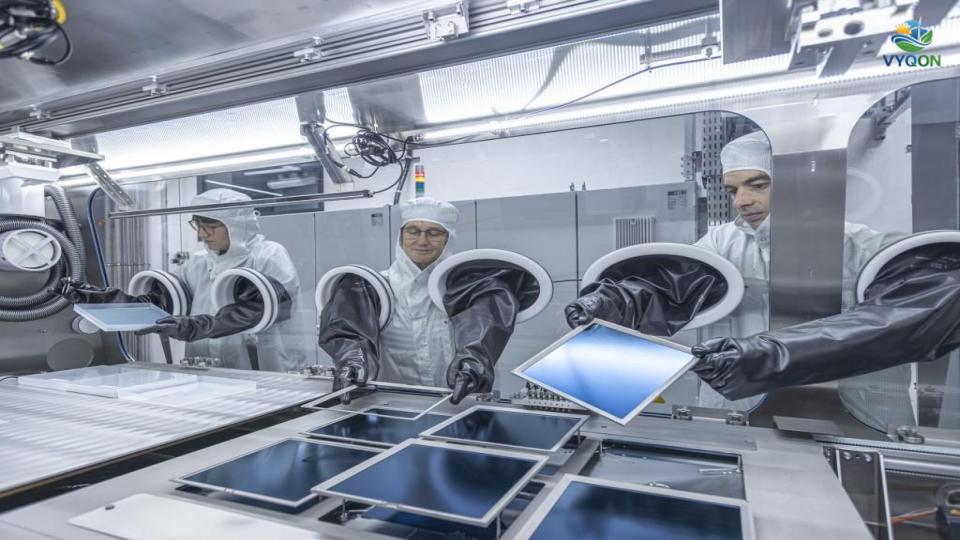
Achieving world records in a highly controlled laboratory environment is vastly different from scaling technology for global, gigawatt-scale manufacturing. To bridge this gap for Perovskite-Silicon Tandem Cells, the Fraunhofer Institute for Solar Energy Systems (ISE) opened a groundbreaking new facility in May 2026.
The facility, named “Pero-Si-SCALE,” provides an independent research and development infrastructure specifically designed to accelerate the market introduction of perovskite-silicon photovoltaics. Previously, laboratory records were often achieved on very small cell areas. The Pero-Si-SCALE laboratory changes this by allowing module manufacturers to transfer these highly complex cell designs to large, industry-standard cell formats up to the G12 wafer size (210 by 210 square millimeters).
By using scalable, high-throughput manufacturing processes such as spatial atomic layer deposition (S-ALD) and highly precise spray coating, this facility is actively solving the coating uniformity and encapsulation challenges that have historically plagued large-area Perovskite-Silicon Tandem Cells.
Why This Architecture Matters for 2026 and Beyond
The transition to Perovskite-Silicon Tandem Cells is not just an academic exercise in efficiency; it holds immense practical value for project developers and engineering, procurement, and construction (EPC) firms globally.
- Maximizing Yield in Space-Constrained Areas: Because these tandem cells generate significantly more watts per square meter, they are the ideal solution for commercial rooftop installations and urban environments where available surface area is strictly limited.
- Lowering the Levelized Cost of Energy (LCOE): Higher module efficiency directly dilutes non-module balance of system (BOS) costs. You need less land, less mounting hardware, and less labor to generate the exact same amount of electricity.
- Leveraging Existing Supply Chains: Because Perovskite-Silicon Tandem Cells use a traditional silicon base, manufacturers do not need to completely abandon their existing silicon infrastructure. They simply add the perovskite coating lines to the end of their current manufacturing process, minimizing extreme capital expenditures.
The Financial and Market Horizon
While leading companies have noted they do not yet have an active mass-production timeline immediately ready for the newly announced 35.5% devices, pilot lines across Europe and Asia are aggressively producing tandem modules right now. The market is rapidly expanding, supported by robust patent portfolios and specialized government funding initiatives.
As we move through the second half of 2026, the global photovoltaic industry is closely watching the progression from G12-sized laboratory prototypes to fully certified, bankable commercial modules. For manufacturers and developers, investing in understanding Perovskite-Silicon Tandem Cells today is non-negotiable for securing market dominance tomorrow.
Official Source References
- PV Magazine (July 15, 2026): Longi sets new world record with 35.5%-efficient perovskite-silicon tandem cell
- LONGi Official Press Release (July 14, 2026): 35.5%! LONGi Once Again Breaks World Record for Crystalline Silicon-Perovskite Tandem Solar Cell Efficiency
- PatSnap Insights (April 2026): Perovskite-silicon tandem solar cells hit 34% in 2026
- Fraunhofer ISE (May 2026): Fraunhofer ISE Opens Laboratory to Accelerate Market Introduction of Perovskite-Silicon Photovoltaics
- Fraunhofer ISE Pero-Si-SCALE Hub (July 2026): Pero-Si-SCALE Facilities and Capabilities
Leave a Comment